The lab facilitates adhesive bonding, contacting, and packaging of bare semiconductor chips. In addition to these tasks, the design, research, and development of new technologies and devices are peformed at this sectoral center.
Main activities
- Design, installation, soldering and repair of complex units such as PCBs, connectors and special applications
- Chip packaging
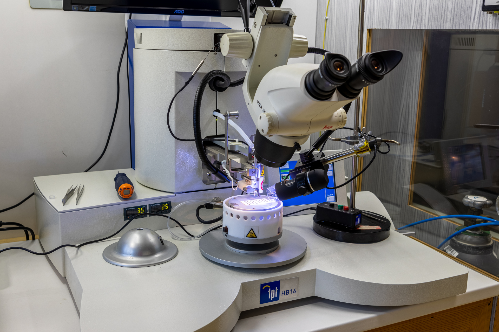
- Contacting of semiconductor chips and other microelectronics using a 0.025-mm Au and AlSi wire and ultrasound, thermocompression or thermosound (ball and wedge technology)
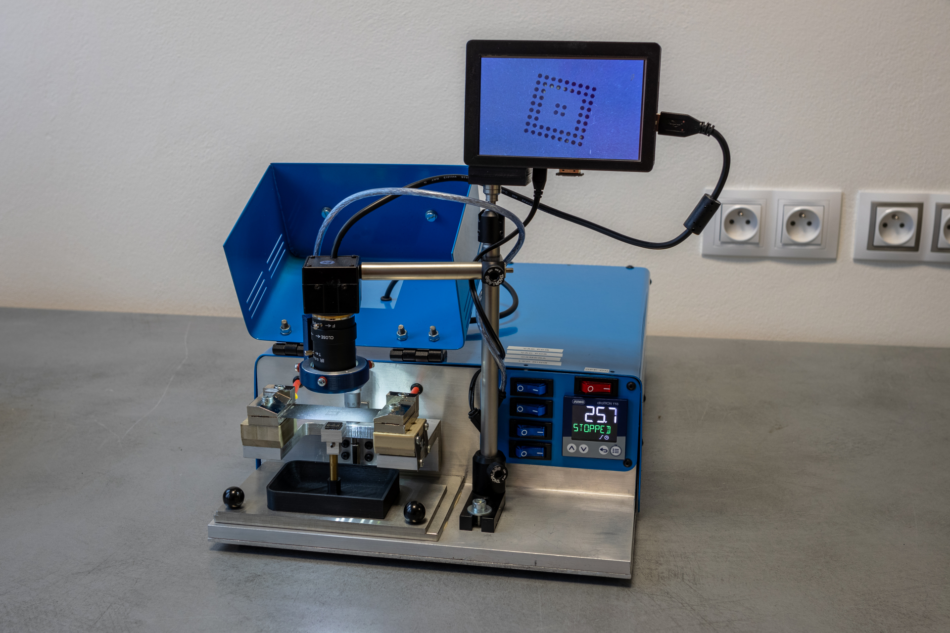
- Printing of viscous materials such as thick-layer pastes and adhesives with a resolution of up to 75 μm and a minimum applied volume of 1nl
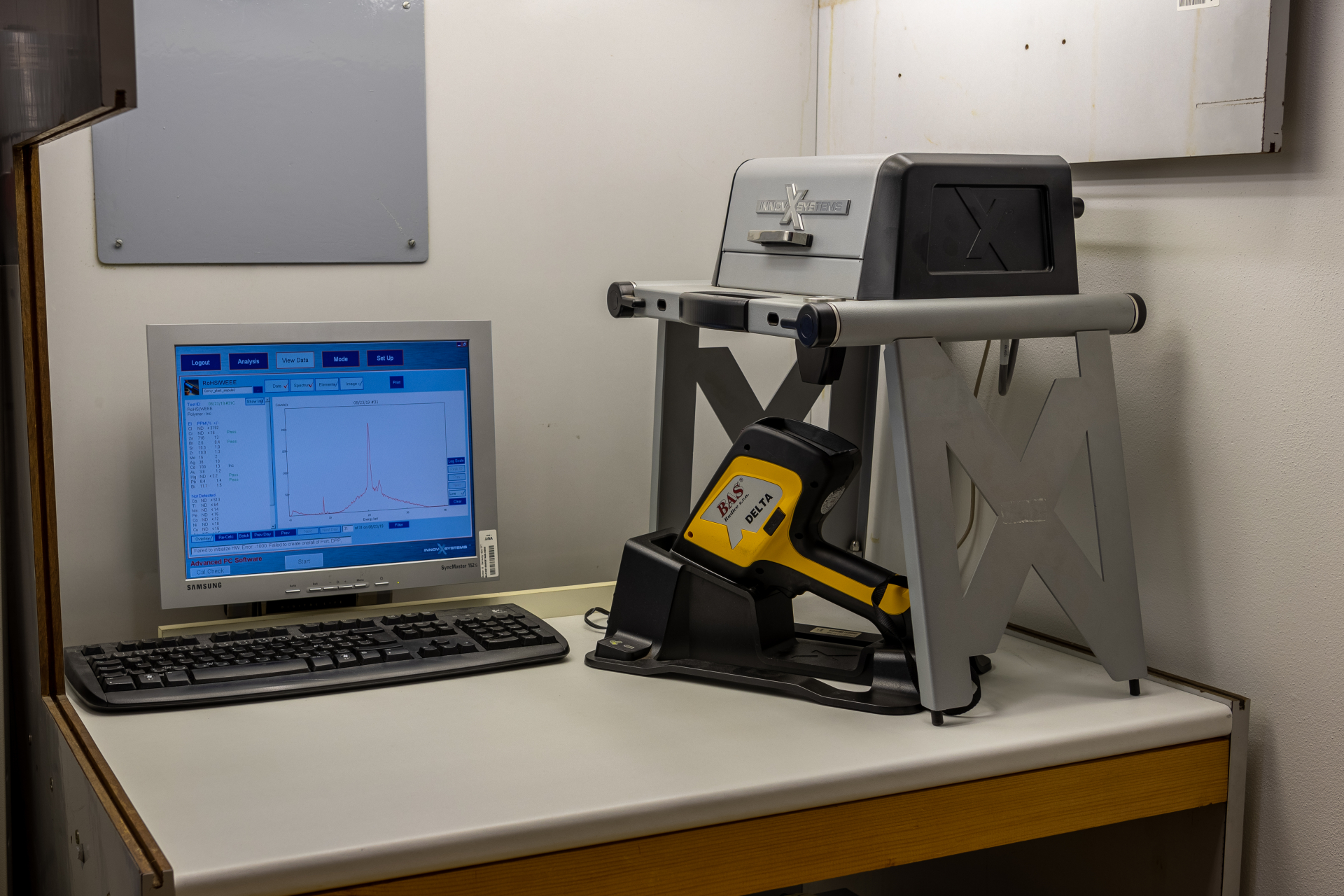
- XRF material analysis
- Metal coating of orifices with a ø up to 0.2 mm in ceramics and glass
- Solving general, practice-related technological problems
- Designing sensor applications to monitor thermodynamic systems, and performing related tasks (such as process monitoring)
Laboratory equipment
- HB 16 semi-automatic wire bonder to perform microwire chip contacting (wedge or ball); stud bumping and ribbon bonding options available
- Dage PC 2400 bond & wire tester to check the tensile and shear strengths in microwires and soldered joints
- U 1202 viscometer
- Olympus XRF Delta material composition analyzer
- In-house designed dispenser to enable viscous material deposition; printing resolution up to 75 µm, depending on the applied material
- Oxygen and hydrogen-fed microburner
- Patent pending stencil for ball attachment or reballing in BGA packages
Responsible person
