Groupleader
Main research areas
- Circuit miniaturization (including lead-free soldering)
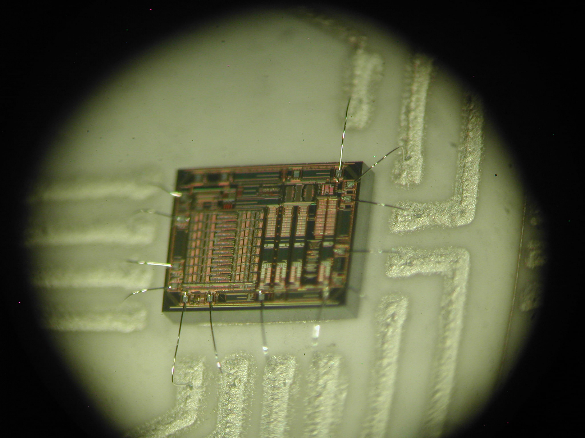
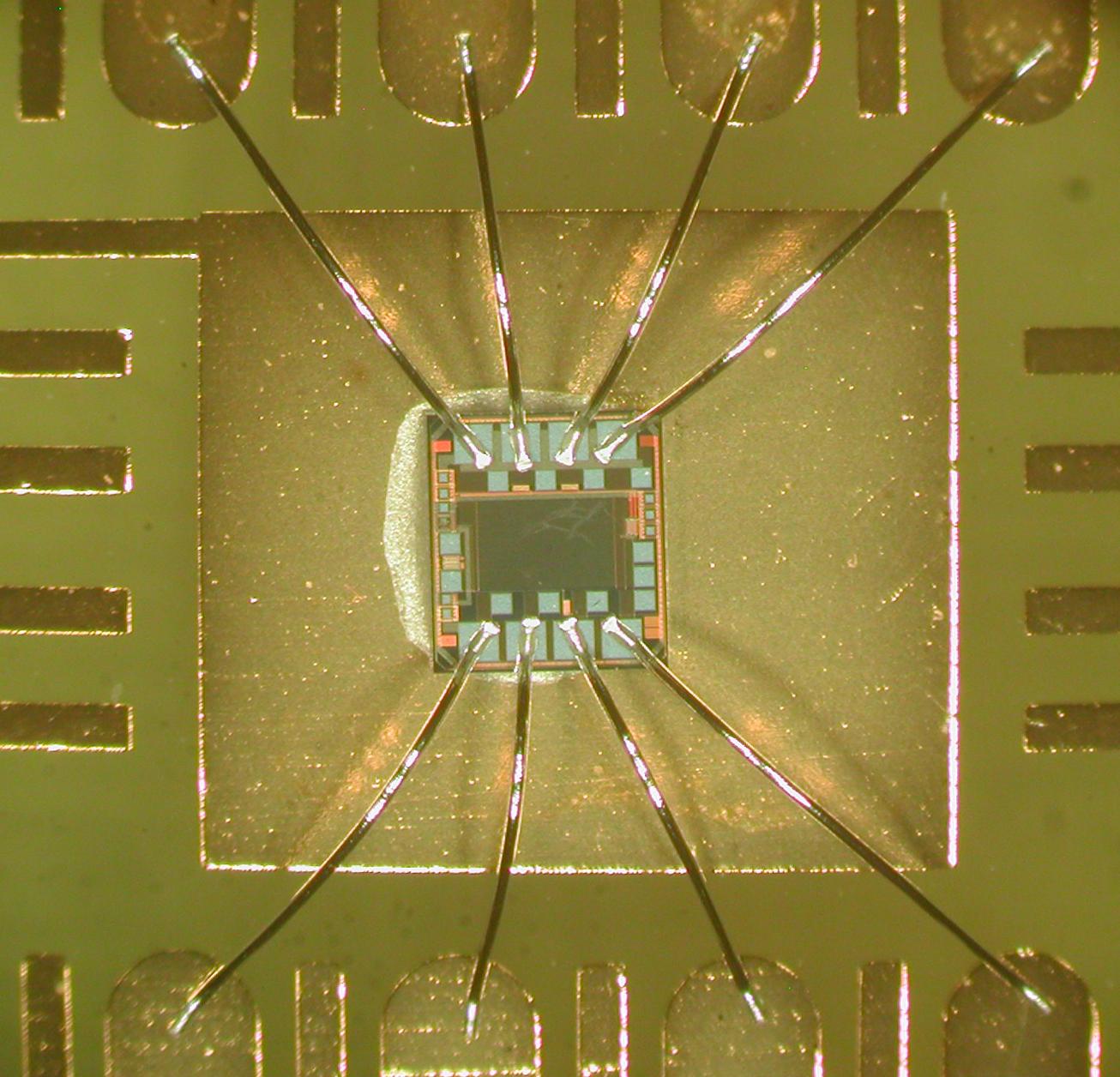
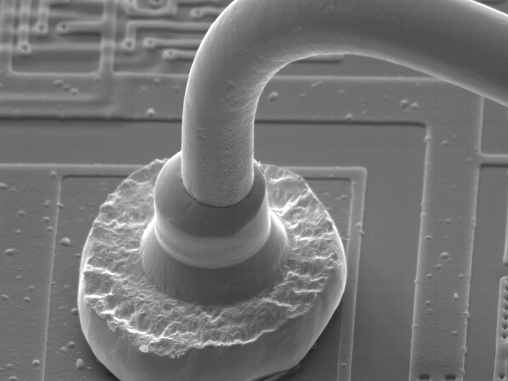
- Semiconductor chip contacting and packaging
- Eco-friendly PCB cleaning
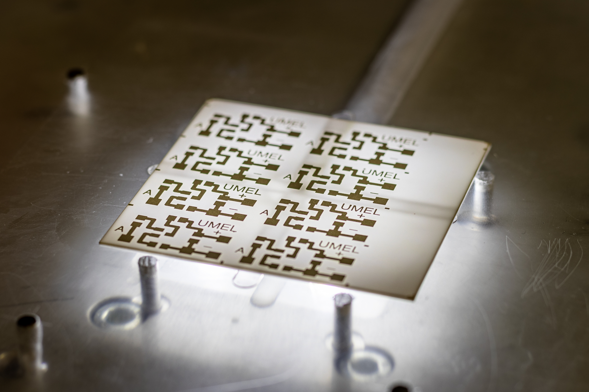
- Multi-layer structures with nested passive components
Main practical research results
- Glass substrates to trace the activity of PBC cleaning agents
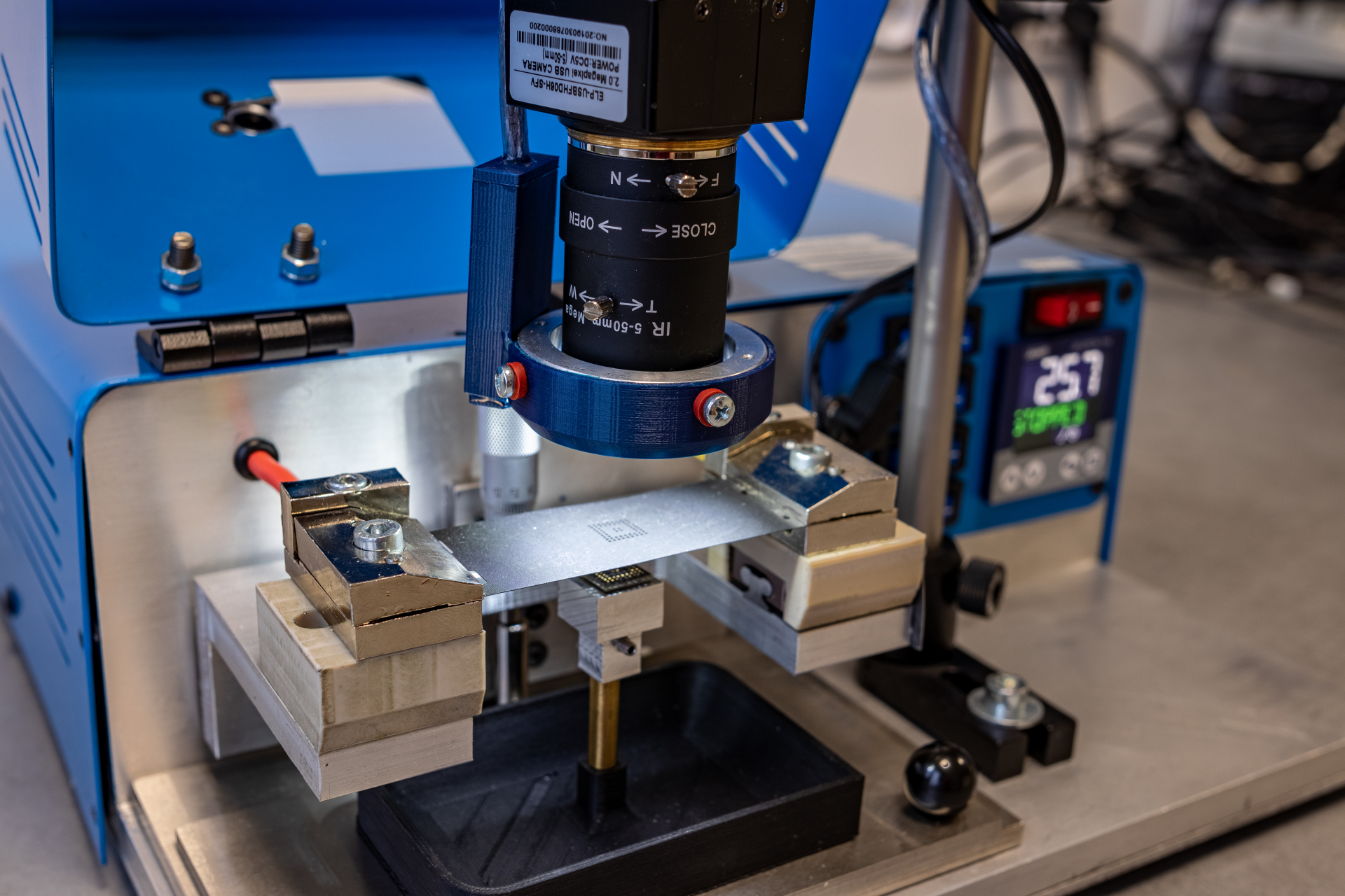
- A directly heated template for re-creating spherical solder outlets in BGA packaging
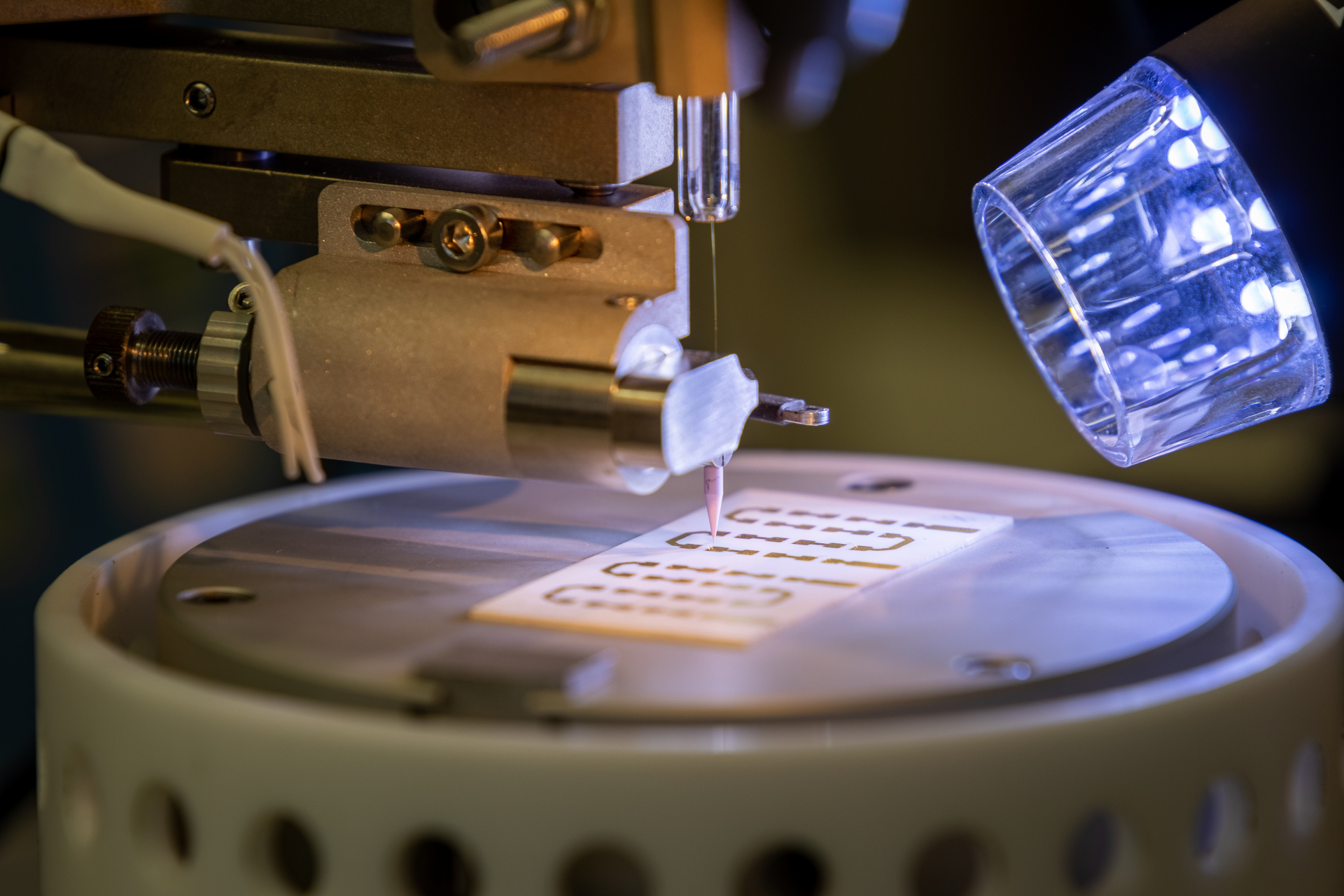
- High-resolution dispensing printing equipment
- A soldering station to operate at reduced pressures in a protective atmosphere
Main research publications
- Šablona pro vytváření pájkových kulových vývodů na pouzdrech BGA
- Influence of heat flow direction on solder ball interfacial layer
- Způsob vytvoření pájkových kulových vývodů na pouzdře elektronické součástky pomocí šablony a šablona k provádění tohoto způsobu
- Acceptability and sensory evaluation of energy bars and protein bars enriched with edible insect
- Dispenzní přístroj pro selektivní nanášení viskózních materiálů
- Welfare of the Mealworm (Tenebrio molitor) Breeding With Regard to Nutrition Value and Food Safety
- Nutritional Potential of Selected Insect Species Reared on the Island of Sumatra
- Moderní mikroelektronické technologie - základ elektronického hardware
- Způsob označování skleněných nebo keramických testovacích desek určených pro náročné aplikace a dispenzer k jeho provádění
- Nanášecí zařízení a způsob vytváření vrstev na vnitřním povrchu malých otvorů
- Ohřevné zařízení s izotermickou topnou plochou
- Nanášecí ústrojí dispenzního přístroje pro selektivní nanášení viskózních materiálů